All visits are free but registration is compulsory (the number of visitors is limited)
| Visit of the company Photline | |
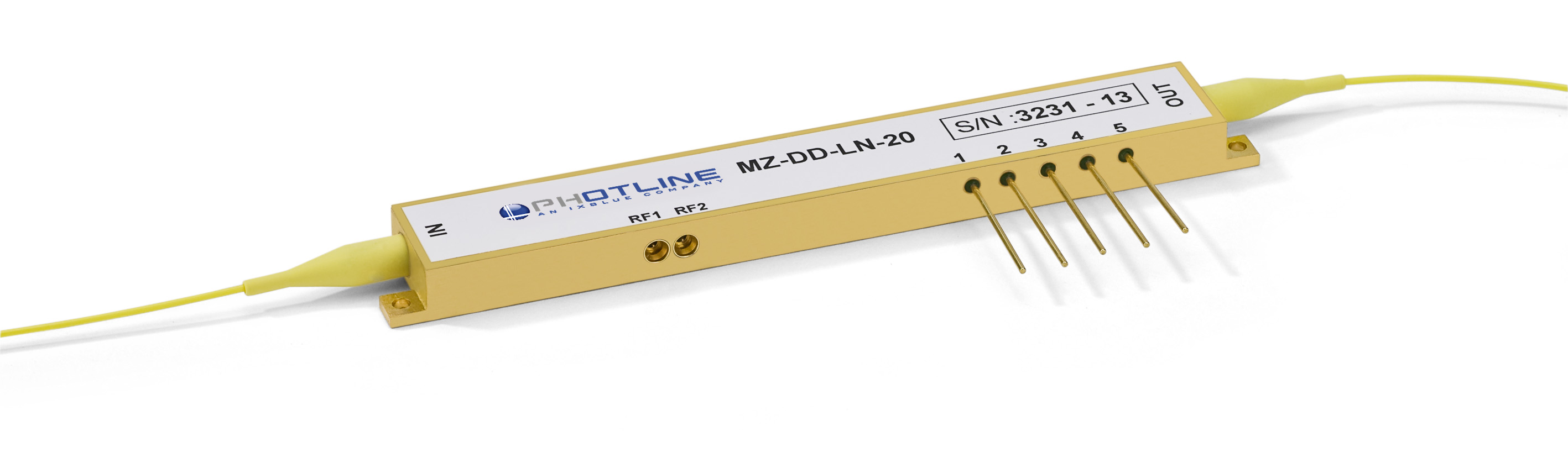
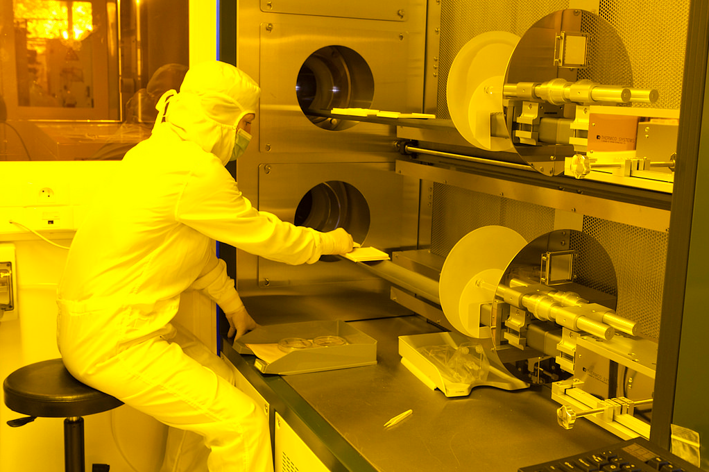
| PHOTLINE (iXBlue, Photonic Solution Division) 3 December 11:05 - 12:00 Five-minute walk from FEMTO-ST - Visit limited to 2*20 people Photline is a leading supplier of optical modulation solutions. The company masters the entire chain of LiNb03 modulators production from computer-assisted design to final characterization, through wafer processing. Markets served by Photline are : Opposite : In the heart of the wafer fab, a class 100 clean room, the multi-tube oven receives wafers for several key stages, including the titanium diffusion process that creates the optical waveguides within the LiNbO3 substrats. This operation requires a very accurate temperature control. © iXBlue, Photonic Solution Division |
lab tour > FEMTO-St
| FEMTO-ST (Franche-Comté Electronics, Mechanics, Thermics and Optics - Sciences and Technologies) 3 December 11:05 - 12:00 or 17:15 - 18:15 Founded in 2004, the FEMTO-ST Institute undertakes research in various scientific disciplines related to engineering, information technology and communication. Its objective is to master micro and nanotechnologies, to develop new devices and systems, to optimize their performance, to provide them with new functions and make them “smart”. |
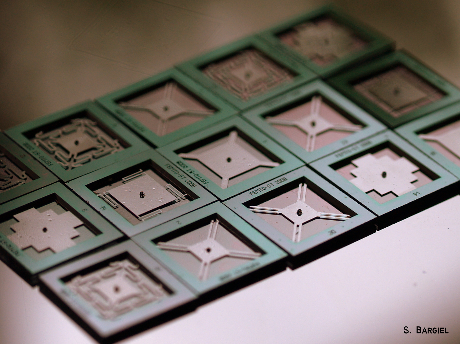
© FEMTO-ST | Micro-and nano structurating of lithium niobate (LN) and tunable photonic crystals Handling areas dedicated to the design and the prototyping of LN ridge waveguides & photonic crystals Visit limited to several groups of 9 people Opposite: Air suspended LN membrane ©FEMTO-ST |
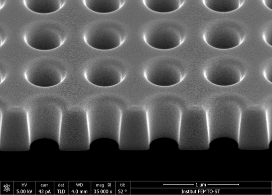
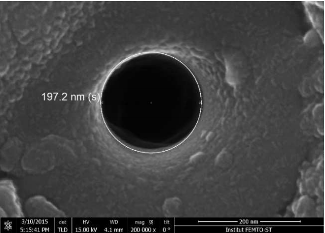
SEM picture © FEMTO-ST | Femtosecond Laser Micro machining Machining, or ablation of matter in the femtosecond regime, in comparison to other machining regimes (picoseconds or nanosecond), allows for a better quality in the structuring of matter. Many applications could be find in the fields of telecommunication, automobile, watchmaking or biomedical fields, as for examples:
Opposite: SEM picture © FEMTO-ST Nano-structuration by Bessel beam in Lithium niobate - New record: Aspect ratio > 2000 A world record for machining: a channel 400nm wide and 43µm long in a thin glass slide |
| MOEMS and optics MIMENTO clearoom facilities (part of the French network RENATECH) Five-minute walk from FEMTO-ST - Visit limited to 2*20 people The FEMTO-ST Institute has several leading edge technological platforms, including the MIMENTO Technology Center. Of national importance, MIMENTO is part of the french RENATECH network which groups together six major academic
Opposite: Z-scanner Set of chips with microlenses © FEMTO-ST / UFC |
![]()